Describe Where Bgas Are Typically Used and Why

A Bga Solder Joint With H 300 Lm A Sem Image Of The Solder Joint Download Scientific Diagram


Pin On Computer Components

Procedure For Preparation Of A Single Bga Structure Joint By Twice Download Scientific Diagram
Bga Void Last Will
Application Note 1126 Bga Ball Grid Array
Ball Grid Array Wikiwand

Ball Grid Array Wikiwand
Xapp426 Implementing Xilnx Flip Chip Bga Packages
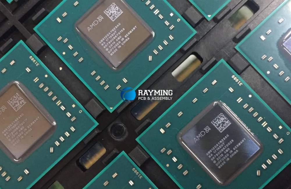
What Is Bga Chip Printed Circuit Board Manufacturing Pcb Assembly Rayming
Bga Land Pattern Design For Manufacturability

A Bga Test Board A 8 Mm Csp And B Bga Test Board B Download Scientific Diagram

A Define Bga Components And Bga Soldering Process Printed Circuit Board Manufacturing Pcb Assembly Rayming
Which Bga Pad And Fanout Strategy Is Right For Your Pcb Blog Altium Designer

Csn33 Micron Bga Manufacturer S User Guide
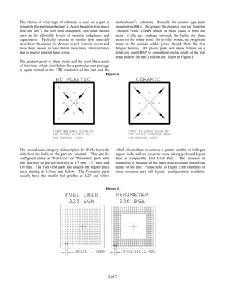
Bga Land Pattern Design For Manufacturability

A Define Bga Components And Bga Soldering Process Printed Circuit Board Manufacturing Pcb Assembly Rayming

Pdf Underfilling Fine Pitch Bgas

A Bga Test Board A 8 Mm Csp And B Bga Test Board B Download Scientific Diagram

A Define Bga Components And Bga Soldering Process Printed Circuit Board Manufacturing Pcb Assembly Rayming

Die Stresses Of Flip Chip Bgas With Underfill A T 142 C And Download Scientific Diagram


Comments
Post a Comment